IOTester® Hardware description.
Introduction to the IOTester concept and the internal I/O devices in the IOTester box
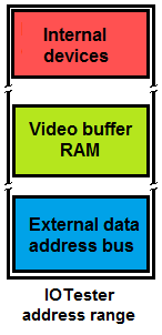
IOTester address range
IOTester implements its own data addressing range, within which the PC program can safely do I/O operations on target hardware, copy I/O data blocks, etc.
The IOTester address range includes the external address bus range, registers for internal devices, and RAM for RGB display controller video memory (type IOTESTER-DISP only).
In this way, an "embedded" I/O device driver can be freely implemented without risk of contention with normal PC hardware.
The internal IOTester address range is always the same, independent of IOTester device configurations.
The part of the address range that is visible on the external connector depends on the IOTester configuration made by the PC program
IOTester pin connector multiplexer
Between the internal IOTester address range and the external IOTester pins is an internal pin multiplexer. The multiplexer configures the pins to be used either as I/O pins (is the power-on default), for external "processor bus" signals, or by special I/O devices in the IOTester box.
In the PC program, groups of connector pins can be configured in one operation simply by enabling internal "I/O devices".
In this way, IOTester can be easily adapted to a wide variety of different I/O target hardware types.
When the External data address bus is enabled, the data bus, WR/RD control, and the lower part of the IOTester address range become visible on external IOTester connector pins.
IOTester box hardware
Description of internal IOTester device functionality and configuration options for IOTester connector pins.
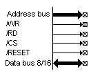
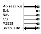
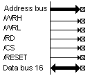
External address / data bus
Pins
Easy connection to I/O chips with a parallel bus processor interface.
Flexible bus pin layout with several selectable layout options for best pin utilization.
Programmable external address bus width: from 0 to 24 pins (16 MB)
Programmable external data bus width: 8 or 16 pins.
Pins not required by the external parallel bus interface configuration are released for use as I/O pins or other devices.
Data bus types
8080 bus type.
8 or 16-bit
6800 bus type.
8 or 16-bit
16-bit with byte
access capability
Bus Chip select,
Multiple /CS,CS
The chip select /CS pin is active (low) whenever the external bus is addressed.
The external address bus holds its state between access operations. Support for data burst type transfers.
The address bus can also emulate an extended chip select multiplexer, providing any combination of active high or active low I/O chip select lines.
Bus Reset
The bus RESET pin is controlled by the PC program (+ toggles automatically low during IOTester power-on).
Full program control of device reset timing and polarity at runtime.
Data block transfers
The external bus supports DMA-like transfer of data blocks from / to the PC. Block transfer can be done with automatic bus address increment, or be done without address increment to provide stream transfer of data blocks to / from the same single bus address. (Stream-like data transfer is supported by most display controllers)
Bus wait states

/RD, /WR or E clock pulse widths can be extended with a programmable number of wait states,
or be extended dynamically on request from an I/O chip via the BUS WAIT pin.
The BUS WAIT input can be rerouted from the default pin to any connector pin not used by other devices.
Port Input-Output
Pins
45 INPUT-OUTPUT port pins are available on the two IOTester target connectors. Any pin not used by the External bus interface, or internal IOTester devices works as an I/O port pin by default.
Reset defaults
After IOTester power-up, all configurable connector pins are INPUT ports, with a weak pull-up, to avoid any contention with target system signals.
I/O pin types
Configurable I/O pin type:
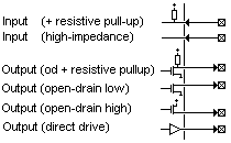
Pins are configured and controlled from the PC via internal IOTester registers - individually or in groups.
Each pin is programmable as input or output. With or without internal pull-up. Outputs can be tri-stated, totem pole, pull-up, or pull-down.
A total of 6 different pin drive modes can be achieved.
Typical I/O-pin-only uses are for: key board scan matrix, LED driver, relay driver, optocoupler interface, etc.
SPI bus device
Pins
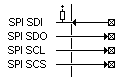
SPI CLK, synchronous clocking of data in or out of slave SPI device
SPI SDO, serial data to slave SPI device
SPI SDI, serial data from slave SPI device
SPI CS, automatic chip select.
The SPI device is configured and controlled from the PC via internal IOTester registers.
Output-only, Input-only, or synchronous Input-Output, SPI CLK polarity. SPI SDO idle states
Multiple SPI data frame sizes: 8-bit (default), 16-bit, 24-bit, or 32-bit, or configurable data frames from 1 to 32 bits.
SPI bus pins not required by the device configuration can be released for use as I/O pins or other devices. SPI pins can be rerouted from the default pins to any connector pin not used by other devices.
SPI master device
Communicates with one or more SPI bus slave devices. SPI slave devices are selected using either the SPI /CS pin (automatic TX/RX data framing), or any IOTester OUTPUT pin not used by other devices. (These /CS pins must be controlled directly by the PC) In this way IOTester can communicate with up to 44 SPI slave devices without the need for SPI address decoding in the target hardware.
Supports DMA-like data block transfer between the SPI TX/RX data register and data blocks on the PC. Automatic data flow synchronization. No risk of SPI device overrun.
I2C bus device
Pins
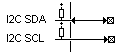
One or more I2C bus slave devices can be connected to the external I2C bus.
I2C pins can be rerouted from the default pins to any connector pin not used by other devices.
I2C master device
The I2C bus master device is accessed and controlled via internal I/O registers.
Fast / slow speed modes. Automatic generation of I2C start and stop signal sequences.
Support for I2C clock-stretching requests from I2C slave devices.
Supports DMA-like data block transfer between the I2C TX/RX data register and data blocks on the PC. Automatic data flow synchronization. No risk of I2C device overrun.
Timestamp counter device
Timestamp device
Internal 32-bit free-running timestamp counter register. No IOTester pins are used.
Incrementing every 1 ms. The counter will wrap to 0 with approx. 49 days interval (unless it is updated in the meantime).
Counter start
The counter is started automatically by the first register read operation (returns 0). No configuration needed.
Can be (re-)started by writing a count start value to the register.
Can be used as a polled timer for the simple generation of accurate timing or delays in the "embedded" PC application.
Can be used as a "stop-watch" for application-controlled timing measurements. Can be used as timestamp mark for profiling.
Timing device
Programmable Counter
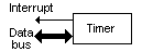
Programmable 16-bit down counter. Decrements every 10 ms. Programmable start value. No IOTester pins are used.
Operates in either "single-count mode", or in "repeated-count mode" with automatic counter reload.
Emulates a typical system clock in an embedded system.
The timer can be configured to generate an interrupt on terminal count to a "Timer interrupt function" in the PC application.
Target Interrupt pin device
Pin
Interrupt input pin. Edge triggered. Secure detection and latch of short interrupt pulses.
To be connected to interrupt lines from external I/O devices, e.g. from an external touch screen controller device.
The pins "interrupt state" can be polled, or can be configured to let events generate an interrupt to an "interrupt pin function" in the PC application.
32 bit pin event counter
An internal 32-bit interrupt event counter counts the number of pulse events detected on the INT0 pin. Can be configured to increment on rising edges or the falling edges.
The counter is started automatically from 0 when the device is enabled. No further configuration needed.
The counter register value can be read directly from the PC. The counter can be (re-)started by writing a count start value to the register.
This event counting operates independent of any interrupt handler settings.
Detection of lost interrupt events
Because the IOTester box operates much faster than a PC can service interrupt events, the event counter register can also be used for lost interrupt detection.
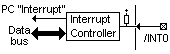
Interrupt controller device
Interrupt device
The interrupt controller routes interrupts from I/O peripherals to the PC for service by "interrupt functions"
in the "embedded" PC application, e.g. from Timer, Interrupt pin, Touch controller.
Provides a common enable / disable of interrupt event generation from devices.
During IDE single step through the PC application, hardware interrupt events are automatically latched for later processing.
IOTester "interrupt" functions
An IOTester interrupt function is any PC application void func(void) function whose address is assigned to the IOTester "interrupt vector table".
"Interrupt" functionality can therefore be debugged with normal PC tools.
This "PC interrupt" facility is intended for use with Human Interface devices.
RGB TFT display controller
In type IOTESTER-DISP
Pin features
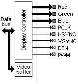
Built-in display controller for RGB TFT, LCD or OLED displays.
Internal video buffer. Directly accessible in IOTester address range.
External 18 or 24-bit RGB bus connections. RGB18 {6:6:6} (J2) or RGB24 {8:8:8} (J2+J1).
Support for RGB16, and other RGB bus widths, via the RGB bus pin connections.
Programmable clocks: Pixel clock, Hsync, Vsync, Data Enable.
Programmable PWM signal pin for display back-light control (0-100% duty-cycle)
The TFT / OLED display controller device in IOTester works in a similar way to those built into many embedded processors.
Programmable display image size up to 1024 x 1024 pixels.
Built-in 16 MB video buffer for image storage. Internal RGB24 color resolution (16MB colors). Automatic conversion to external RGB bus color resolution.
The content of the internal video buffer RAM is operated as one linear I/O register array.
The video buffer can be used with DMA-like data block transfer from / to data blocks on the PC.
Support for multiple frame buffers. Fast swap between image buffers. Flicker-free update.
Built-in fill and copy accelerator. Supports operations on Linear buffers, rectangular blocks in a buffer (sprites), and single register streams.
Copies data between buffers in internal video RAM, between buffers and the external bus, or between buffers and SPI, I2C buses
Touch screen device
In type IOTESTER-DISP
Pins
Touch detection
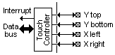
Built-in touch screen controller for a 4-wire resistive touch screen.
Detects relative X, Y positions for touch position on screen.
Detects touch-down, touch-drag, and touch-up events. Each event type can be configured to generate an interrupt to a "touch screen interrupt function" in the PC application.
The touch screen device in IOTester works in a similar way to those built into many embedded processors.
Target Power supply
Built-in 3V3 power supply regulator
Small target systems connected to IOTester can be supplied from IOTester via the target interface connectors, e.g. small display modules.
Only USB connection to PC: 3V3 300mA regulated
With Power Adaptor connected: 3V3 800mA regulated, plus 5V 1A. 5V pin is connected directly to the DC adaptor
Tough target interface
All pins are 5V tolerant and can directly interface to 5V logic.
All pins are EMC, over-voltage, under-voltage, and short-circuit protected.
DC input up to 8V. Reverse voltage protected. 3V3 regulator is over-current and over-temperature protected.